I’m a manufacturing/electronics/design/theory mentor on a FIRST Robotics team. The last six weeks have literally been a blur. This post is a sleep-deprived ramble.
You’ve been warned.
I wake up at 5am to get ready for work, I head over to the high school for 4pm, and then I’m back home in bed for 11pm. Wash, rinse, repeat.
And I love it.
I love that the students are excited. I love that year after year after year, they surprise me. I love that the alumni come back and help out with the newbies, themselves turning into leaders with the new batch of newbs the following year. These kids are getting an experience I never had. These kids have never had people work with them some closely before in their lives. These kids have ideas that matter, working on a project that challenges many a masters student.
I’ve seen mentors from the local universities show up, take a week or two off, and come back with a ‘solution’ they had to a problem we experienced the last time they were there, only to be blown away at the progress. ‘Oh yea, that thing we had that issue with? We scrapped the whole design the next day. This is our fourth iteration. Welcome to FIRST.’
Seeing grade nine students blow the pants off of senior engineering students is a thing of real beauty.
Anyways, the Tek 7854 ROM board redesign has been woven between those precious minutes between ‘rinse’ and ‘repeat.’ I’ve ransacked my personal library, pulling out all my digital design texts to try and jumpstart the librarian in my mind-palace.
I sat one night and seriously thought about what I wanted to do. I want to fix my oscilloscope. I want it to work. I want to love it and to squeeze it and to call it George. I pulled out the service manual I’ve found and polled the internet for information. Quickly I found that the ROM board I had, developed in the ’70s, varied vastly from the one designed in 1989 (and why not). Where my ROM board had four flash chips and a special flash chip that stored the lookup table, the revised board had only two chips with the image and no ‘decoder ring.’ Furthermore where my oscilloscope has 43 chips on its RAM board, the revised version has only two SRAM chips.
Both boards share address and data busses, both board have buffers, both boards have supporting CS logic chips, and both boards have local voltage regulators. The revised oscilloscope has a single board, with a single set of buffers, a single set of support logic ICs, and a single set of V-regs. This is all stuffed onto the A28 RAM card, leaving the position occupied for the original ROM card open.
Ok, so, in my oscilloscope there are four ROM ICs, organized in pairs; the first two ROMs storing data from address 0 to 7, and the second pair storing data from address 8 to 15. The CPU is a TI TMS9900 and the memory addressing layout is organized as shown:
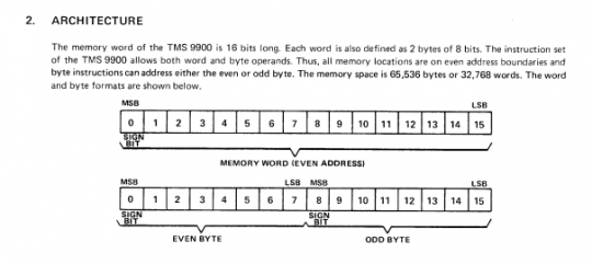
So one pair of chips stores the even bytes, and the other pair, the odd. The CPU basically sees this, from what I understand:
The 8-bit odd byte file might have data:
x00 0101 0101
x01 0010 0010

And the 8-bit even byte file might have data:
x00 1010 1010
x01 1101 1101

So, the combined 16-bit file would look like this:
x00 1010 1010 0101 0101
x01 1101 1101 0010 0010
I think I can make a single file from two ROM images, keeping the hardware simple, and the software flexible. I had a couple Teensy 3.0 uCs on hand, and two Teensy 3.1 uCs on the way. Next step is to try and see if I can load my merged ROM image onto one of these uCs, hijack the data and address lines, and see if I can get my oscilloscope to kick. I’ll make up a script to fold the images into one another.
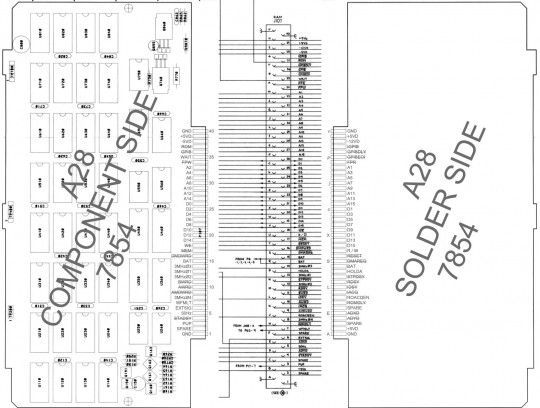
I’ll need to develop my own PCB, because why not. Unfortunately I couldn’t find what the edge connector pinout was. This was simple enough to figure out; here are my findings:
The next steps are to sit down and create a custom part in Eagle PCB, or maybe give KiCAD a try. Here is a terrible CAD representation of the somewhat odd dimensions I’m dealing with:
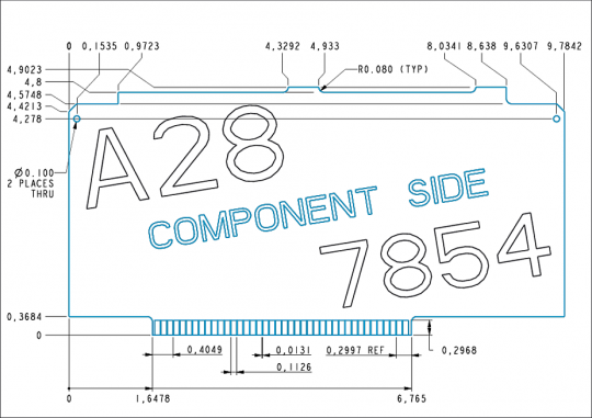
The units are inches (ignore the extra digits), but some of the numbers translate to metric quite nicely (9.7842 ~=248.5mm, 4.9023 ~= 124.5mm, 0.080″ = 2.0mm, 0.2968 ~= 7.5mm) while others, such as the tabs on the top, don’t ( 4.933″ – 4.3292″ ~= 15.336mm, 8.638″ – 8.0341″ ~= 15.339mm; they’re close, so that’s nice at least).
Hopefully I’ll have this part made up in the next week or two (I’ve only accumulated an hour or two worth of time to work on this over the last week) and I’ll be able to cut a prototype board at work.
So, that’s where my life is right now.
If the women don’t find you handsome, they should at least find you handy.